Electronic / Semiconductor

Nanoray Co. has X-Ray energy spectroscopy technology, widely used in electronic / semiconductor, energy / material, food / pharma, academic / project.
Technical capabilities synchronize to international standards, and there is radiation safety certification.

Electronic / Semiconductor

Nanoray’s intelligent detection advantages, excellent imaging quality and intelligent detection technology are widely used in SMT, FPC, PCB, Chip, passive components, etc.

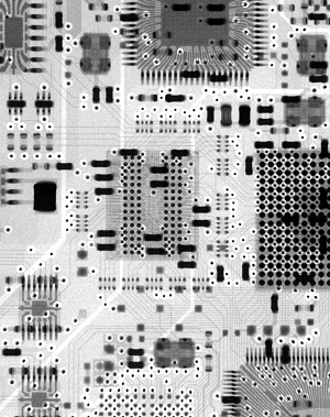
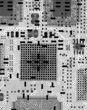
Detection application – Xray principle is used for perspective detection, which is mainly used in BGA bubble detection, empty welding, cold welding, short circuit/open circuit, internal crack, foreign body detection, angle deviation, multiple/missing parts, abnormal appearance, etc. can be inspected.

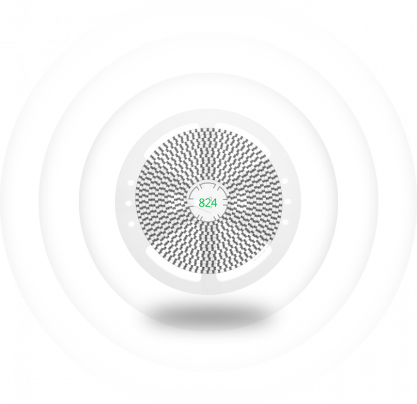
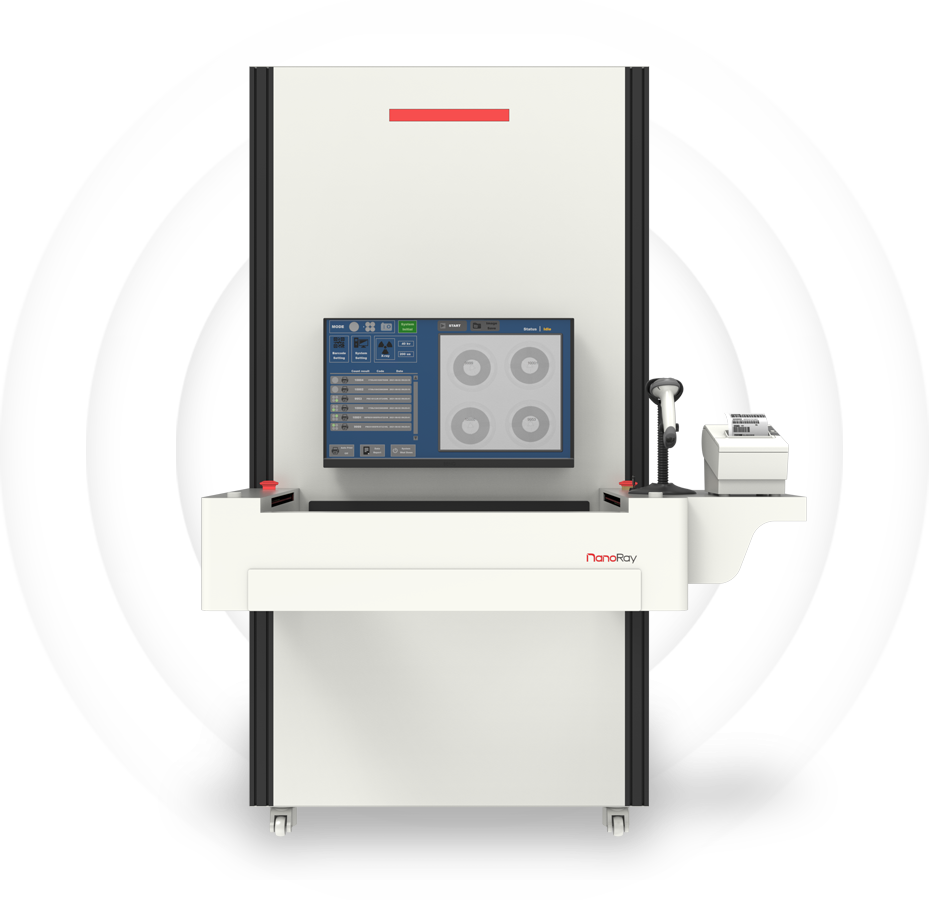
SMD component counting machine

Technical advantages and characteristics:

  • Fast detection, 12 seconds/Pcs
  • Four pieces can be tested at a time to achieve the outcome of economization on man power.
  • Detection range: maximum diameter is up to 430mm
  • Intelligent equipment with bar code machine and data management provides the real-time feedback in series with MES.
  • Excellent optical design, superior image quality, false positive rate less than 0.01%
  • The minimum detectable value is 01005 and other small materials

Printed Circuit Board, PCB

  • PCB (Printed Circuit Board) is the mother of the industry. Up to the present day, most of the circuit boards are attached with an etching inhibitor which are etched after exposure and development then the penetration image technology is used to observe those exposure and development .
  • Detectable items include drilling location, hole size, burr, open circuit and short circuit.

Surface-mount technology,SMT

  • SMT(Surface Mount Technology) forms component connection through soldering. The traditional detection method is using probe electrical measurement and AOI detection. However, the improvement of product precision , the reduction of electronic components and the circuit Assembly quality requirements are also getting strict along with the development of packaging technology. X-Ray penetration testing technology is becoming more popular and can not only detect invisible solder joints but also further analyze the test results to understand the situation during the process.
  • Detectable items include solder thickness, size, uniformity, offset, missing parts, air bubbles, less tin, empty soldering/virtual soldering and solder bridges/tin whiskers.

ball grid array (BGA)

  • BGA(Ball Grid Array) welding is an important processing process in PCBA. The quality of welding will affect the defect-free rate and stability of the finished product. However, because the inspection after BGA welding is difficult, X-Ray penetration inspection technology is required to ensure the quality of the welding process.
  • Detectable items include air bubbles, short circuits, open circuits, displacement, air-cooled soldering, solder ball integrity.

INDUSTRIAL INSPECTION

Applications

Nanoray Co. has X-Ray energy spectroscopy technology, widely used in electronic / semiconductor, energy / material, food / pharma, academic / project.
Technical capabilities synchronize to international standards, and there is radiation safety certification.
電子半導體

Electronic / Semiconductor

能源材料

Green Energy / Material

食安藥檢

Food / Pharma Safety

學研專案

Academic / Project